- 您现在的位置:买卖IC网 > Sheet目录3818 > PIC18F4580-I/PT (Microchip Technology)IC PIC MCU FLASH 16KX16 44TQFP
MCP2515
DS21801F-page 42
2010 Microchip Technology Inc.
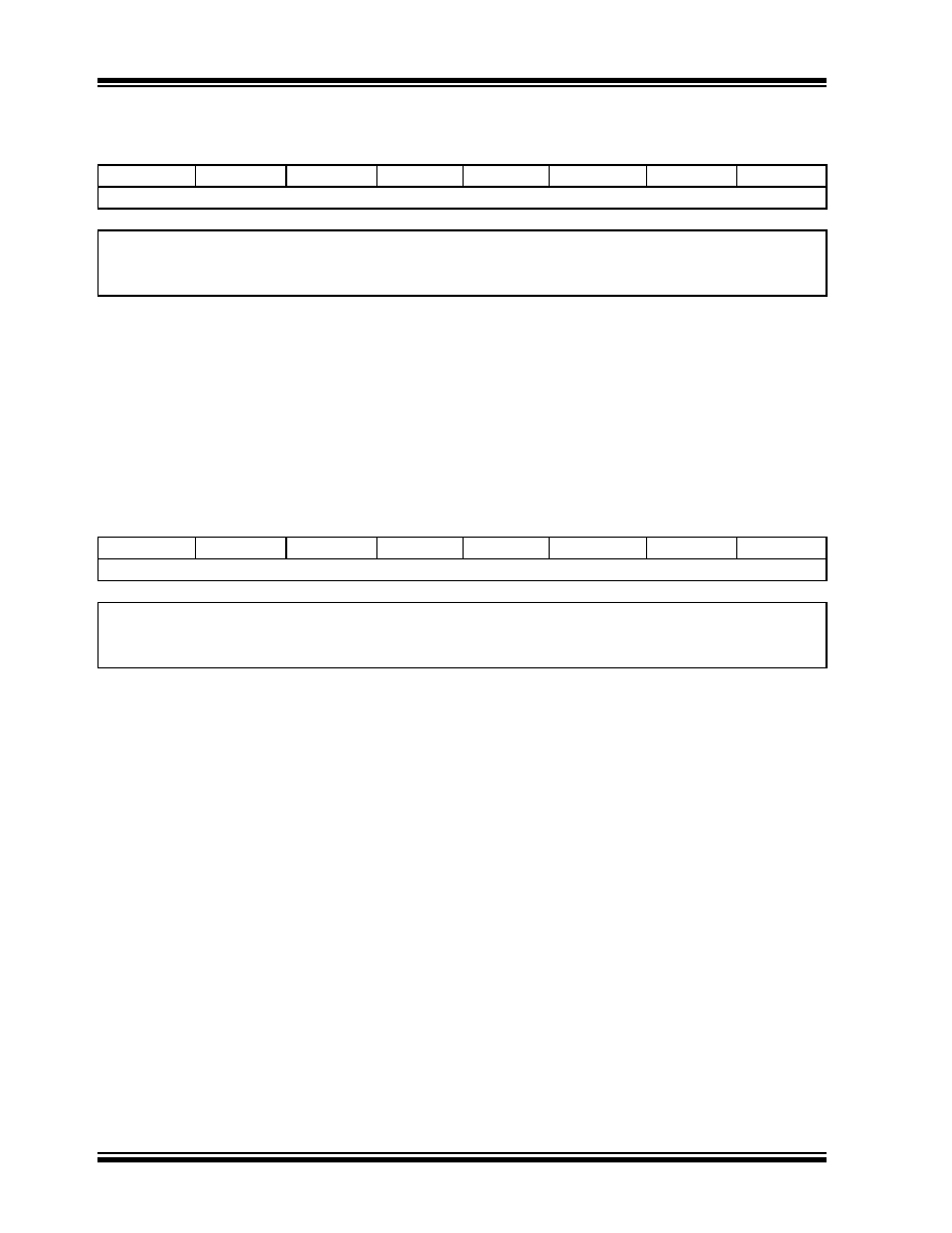
REGISTER 5-1:
CNF1 – CONFIGURATION 1 (ADDRESS: 2Ah)
R/W-0
SJW1
SJW0
BRP5
BRP4
BRP3
BRP2
BRP1
BRP0
bit 7
bit 0
Legend:
R = Readable bit
W = Writable bit
U = Unimplemented bit, read as ‘0’
-n = Value at POR
‘1’ = Bit is set
‘0’ = Bit is cleared
x = Bit is unknown
bit 7-6
SJW: Synchronization Jump Width Length bits <1:0>
11
= Length = 4 x TQ
10
= Length = 3 x TQ
01
= Length = 2 x TQ
00
= Length = 1 x TQ
bit 5-0
BRP: Baud Rate Prescaler bits <5:0>
TQ = 2 x (BRP + 1)/FOSC
REGISTER 5-2:
CNF2 – CONFIGURATION 1 (ADDRESS: 29h)
R/W-0
BTLMODE
SAM
PHSEG12
PHSEG11
PHSEG10
PRSEG2
PRSEG1
PRSEG0
bit 7
bit 0
Legend:
R = Readable bit
W = Writable bit
U = Unimplemented bit, read as ‘0’
-n = Value at POR
‘1’ = Bit is set
‘0’ = Bit is cleared
x = Bit is unknown
bit 7
BTLMODE: PS2 Bit Time Length bit
1
= Length of PS2 determined by PHSEG22:PHSEG20 bits of CNF3
0
= Length of PS2 is the greater of PS1 and IPT (2 TQ)
bit 6
SAM: Sample Point Configuration bit
1
= Bus line is sampled three times at the sample point
0
= Bus line is sampled once at the sample point
bit 5-3
PHSEG1: PS1 Length bits<2:0>
(PHSEG1 + 1) x TQ
bit 2-0
PRSEG: Propagation Segment Length bits <2:0>
(PRSEG + 1) x TQ
发布紧急采购,3分钟左右您将得到回复。
相关PDF资料
PIC16C76-20/SO
IC MCU OTP 8KX14 A/D PWM 28SOIC
PIC16F874-20I/P
IC MCU FLASH 4KX14 EE 40DIP
PIC16C76-10/SP
IC MCU OTP 8KX14 A/D PWM 28DIP
PIC16C76-20/SP
IC MCU OTP 8KX14 A/D PWM 28DIP
PIC18F2580-I/ML
IC PIC MCU FLASH 16KX16 28QFN
PIC16LF877A-I/L
IC MCU FLASH 8KX14 EE A/D 44PLCC
PIC32MX340F256H-80V/PT
IC MCU 32BIT 256KB FLASH 64TQFP
PIC18F4553-I/PT
IC PIC MCU FLASH 16KX16 44TQFP
相关代理商/技术参数
PIC18F4580-I/PT-ND
制造商: 功能描述: 制造商:undefined 功能描述:
PIC18F4580T-I/ML
功能描述:8位微控制器 -MCU 32 KB FL 1536 RAM 36 I/O RoHS:否 制造商:Silicon Labs 核心:8051 处理器系列:C8051F39x 数据总线宽度:8 bit 最大时钟频率:50 MHz 程序存储器大小:16 KB 数据 RAM 大小:1 KB 片上 ADC:Yes 工作电源电压:1.8 V to 3.6 V 工作温度范围:- 40 C to + 105 C 封装 / 箱体:QFN-20 安装风格:SMD/SMT
PIC18F4580T-I/PT
功能描述:8位微控制器 -MCU 32 KB FL 1536 RAM 36 I/O RoHS:否 制造商:Silicon Labs 核心:8051 处理器系列:C8051F39x 数据总线宽度:8 bit 最大时钟频率:50 MHz 程序存储器大小:16 KB 数据 RAM 大小:1 KB 片上 ADC:Yes 工作电源电压:1.8 V to 3.6 V 工作温度范围:- 40 C to + 105 C 封装 / 箱体:QFN-20 安装风格:SMD/SMT
PIC18F4585-E/ML
功能描述:8位微控制器 -MCU 48KB 3328 RAM w/ECAN RoHS:否 制造商:Silicon Labs 核心:8051 处理器系列:C8051F39x 数据总线宽度:8 bit 最大时钟频率:50 MHz 程序存储器大小:16 KB 数据 RAM 大小:1 KB 片上 ADC:Yes 工作电源电压:1.8 V to 3.6 V 工作温度范围:- 40 C to + 105 C 封装 / 箱体:QFN-20 安装风格:SMD/SMT
PIC18F4585-E/P
功能描述:8位微控制器 -MCU 48KB 3328 RAM w/ECAN RoHS:否 制造商:Silicon Labs 核心:8051 处理器系列:C8051F39x 数据总线宽度:8 bit 最大时钟频率:50 MHz 程序存储器大小:16 KB 数据 RAM 大小:1 KB 片上 ADC:Yes 工作电源电压:1.8 V to 3.6 V 工作温度范围:- 40 C to + 105 C 封装 / 箱体:QFN-20 安装风格:SMD/SMT
PIC18F4585-E/PT
功能描述:8位微控制器 -MCU 48KB 3328 RAM w/ECAN RoHS:否 制造商:Silicon Labs 核心:8051 处理器系列:C8051F39x 数据总线宽度:8 bit 最大时钟频率:50 MHz 程序存储器大小:16 KB 数据 RAM 大小:1 KB 片上 ADC:Yes 工作电源电压:1.8 V to 3.6 V 工作温度范围:- 40 C to + 105 C 封装 / 箱体:QFN-20 安装风格:SMD/SMT
PIC18F4585-H/ML
功能描述:8位微控制器 -MCU 48 KB Flash 3328 RAM 36 I/O w/ECAN RoHS:否 制造商:Silicon Labs 核心:8051 处理器系列:C8051F39x 数据总线宽度:8 bit 最大时钟频率:50 MHz 程序存储器大小:16 KB 数据 RAM 大小:1 KB 片上 ADC:Yes 工作电源电压:1.8 V to 3.6 V 工作温度范围:- 40 C to + 105 C 封装 / 箱体:QFN-20 安装风格:SMD/SMT
PIC18F4585-H/P
功能描述:8位微控制器 -MCU 48 KB Flash 3328 RAM 36 I/O w/ECAN RoHS:否 制造商:Silicon Labs 核心:8051 处理器系列:C8051F39x 数据总线宽度:8 bit 最大时钟频率:50 MHz 程序存储器大小:16 KB 数据 RAM 大小:1 KB 片上 ADC:Yes 工作电源电压:1.8 V to 3.6 V 工作温度范围:- 40 C to + 105 C 封装 / 箱体:QFN-20 安装风格:SMD/SMT